
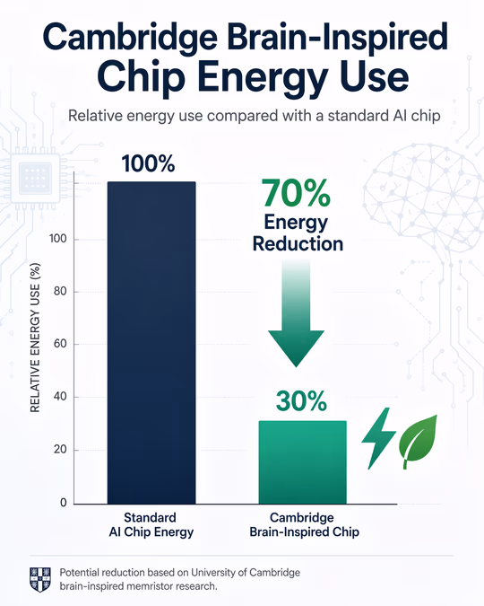
New Brain-Inspired Chip Could Slash AI Energy Use by 70%
Cambridge researchers develop a hafnium oxide memristor that mimics neurons, potentially cutting AI energy consumption by 70%.
Researchers at the University of Cambridge have engineered a nanoelectronic device that mimics the human brain’s architecture, potentially reducing the energy consumption of artificial intelligence hardware by up to 70%. By utilizing a modified form of hafnium oxide, a material already common in the semiconductor industry, the team created a 'memristor' that combines data storage and processing in a single location.
This breakthrough, recently published in the journal Science Advances, addresses the most significant hurdle in modern computing: the von Neumann bottleneck. In traditional computer architectures, the memory unit and the processing unit are physically separate. This design necessitates a constant, power-hungry transfer of data between the two components. As AI models grow in complexity, this 'memory wall' leads to escalating electricity costs and environmental concerns.

Mimicking the Biological Synapse
The human brain operates with an efficiency that modern silicon struggles to match. It performs approximately 10^14 synaptic operations per second while consuming only about 20 watts of power. It achieves this by storing and processing information simultaneously at its synapses. The Cambridge team’s device, led by Dr. Babak Bakhit from the Department of Materials Science and Metallurgy, replicates this by functioning as a memristor—a component that 'remembers' the amount of charge that has previously flowed through it.
"Energy consumption is one of the key challenges in current AI hardware," said Dr. Bakhit. "To address that, you need devices with extremely low currents, excellent stability, outstanding uniformity across switching cycles and devices, and the ability to switch between many distinct states."
The researchers achieved this by enriching a hafnium oxide thin film with strontium and titanium. Unlike previous memristors that relied on unpredictable 'filamentary' mechanisms—where thin conductive paths form and break at random—this new device utilizes p-n junctions at its interfaces to smoothly change resistance.
Dr. Bakhit noted that while filamentary devices suffer from random behavior, their new devices switch at the interface, allowing for outstanding uniformity from cycle to cycle and device to device. In laboratory testing, the chips demonstrated hundreds of distinct, stable conductance levels, a prerequisite for the analogue 'in-memory' computing required for sophisticated neural networks.
Ultra-Low Power and Industrial Potential
The performance metrics of the new device are striking. The Cambridge team reported switching currents approximately a million times lower than some conventional oxide-based memristors. During experiments, the devices remained stable through tens of thousands of switching cycles and retained their programmed states for approximately 24 hours.
One of the most promising aspects of this research is the choice of material. Hafnium oxide is already a standard component in advanced CMOS transistors used in today’s smartphones and laptops. This existing familiarity could significantly ease the transition from the laboratory to industrial manufacturing, as the materials are already compatible with current semiconductor fabrication lines.
However, the path to commercialization is not without obstacles. Dr. Bakhit mentioned that the team faced thousands of failures and struggled for nearly three years before identifying the current optimal technology parameters. A significant remaining challenge is the fabrication temperature; currently, the multicomponent films require around 700°C. This is considerably higher than the temperatures allowed in standard semiconductor back-end-of-line processing.

The Road Ahead for Sustainable AI
The implications of a 70% energy reduction are profound for the future of the AI industry. As data centers continue to strain power grids and the demand for edge AI—intelligence processed locally on devices like smartwatches or sensors—increases, power efficiency has become as critical as raw processing speed.
Dr. Bakhit is now focused on bringing the required fabrication temperature down to make the technology more palatable for high-volume manufacturing. If successful, this brain-inspired hardware could move AI beyond the limits of traditional silicon architecture, enabling more sustainable, cost-effective, and adaptable machine learning systems. By integrating memory and processing, the technology moves us one step closer to hardware that truly reflects the elegance and efficiency of biological intelligence.